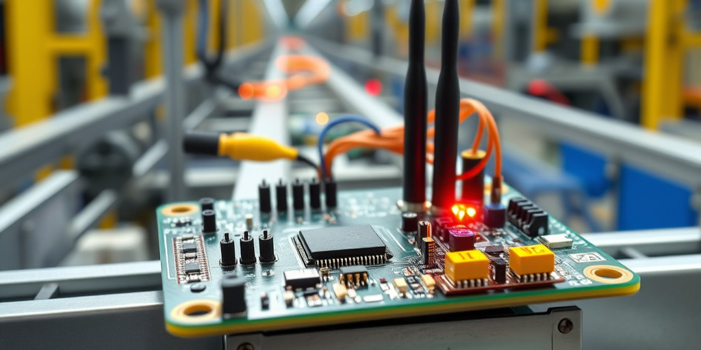
What Makes a PCB an "HDI" Board?
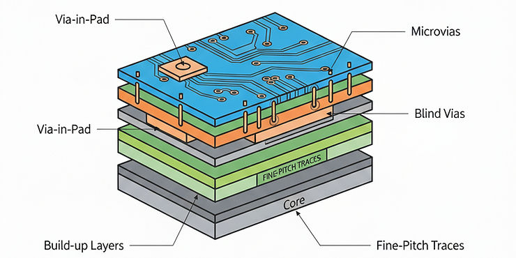
Think of HDI as an evolution of the traditional multilayer PCB. It’s all about creating more connections in a smaller area using advanced techniques. The key is to use build-up layers and tiny microvias to achieve a much higher wiring density.
Here’s a breakdown of the core building blocks:
-
Microvias: These are tiny, laser-drilled holes (typically 75–150 µm) that connect one layer of the board to the next. They're much smaller than the mechanical drills used for standard vias.
-
Blind and Buried Vias: Instead of running all the way through the board, these vias connect an outer layer to an inner one (blind) or two inner layers to each other (buried). This saves space and keeps the board cleaner.
-
Sequential Lamination: This is the process of adding layers one by one to create the microvia connections. You can have a 1-n-1 stackup with one build-up layer on each side, a 2-n-2 with two layers, or even any-layer HDI, where microvias can connect any adjacent layers for ultimate density.
-
Via-in-Pad & copper fill: This technique places microvias directly inside the pads of fine-pitch components like BGAs. The vias are then filled and capped, creating a perfectly flat surface for soldering. This frees up routing space and improves signal integrity.
The result is a board with finer lines and spaces, shorter stubs, and improved signal quality, all in a much smaller package.
When to Choose HDI for Your Industrial System
You don’t need an HDI board for every project. They are best suited for applications where standard PCBs just can't keep up.
-
You're dealing with tight spaces: If your design has strict size and weight limits, such as in smart sensors or compact edge controllers, HDI is the perfect solution.
-
You're working with high-speed or mixed signals: For systems with fast data links, like SERDES, or high-precision components, HDI helps maintain signal integrity and reduces electromagnetic interference (EMI).
-
Your board has complex, high-density components: Escaping signals from fine-pitch BGAs (0.5 mm or less) can be a nightmare on standard boards. HDI makes this process much more manageable.
-
Reliability in harsh environments is a must: Shorter, more direct connections and robust materials give HDI boards an edge when dealing with thermal stress and vibration.
The Building Blocks
Vias & Stackups
-
Microvia aspect ratio is typically kept low (≈1:1 or less) for better plating and fatigue life.
-
Staggered vs. stacked: Staggered microvias tend to be more robust under thermal cycling; stacked saves area but needs filled/capped plating done right.
-
Common stackups:
-
1-n-1 HDI: One build-up layer per side; good for moderate density.
-
2-n-2 HDI: Two build-ups per side; more escape options for fine-pitch BGAs.
-
Any-layer HDI: Microvias between any adjacent layers; maximum density, highest cost.
-
Materials
-
High-Tg FR-4 derivatives (for -40 °C to +105/+125 °C ranges), with low CTE for microvia reliability.
-
Low-loss dielectrics when signal integrity matters (lower Dk/Df improves eye margins).
-
Halogen-free options for environmental/industry requirements.
Copper & Finishes
-
Balanced copper reduces warpage in reflow and improves dimensional stability.
-
Surface finishes: ENIG/ENEPIG for fine-pitch and wire-bond options; LF-HASL for cost but not ideal for very fine pads.
Key Considerations for Industrial-Grade High-Density Interconnect PCBs
Industrial environments are demanding, so it's not enough for an HDI board to just be "dense." It also has to be tough.
Electrical Performance:
-
Better Signals: Microvias eliminate long stubs, which are a major cause of signal degradation in high-speed designs.
-
Cleaner Return Paths: Blind vias and controlled impedance planes help manage signals and reduce EMI.
-
Lower Noise: Short, direct connections reduce parasitic inductance, which helps with decoupling around high-speed ICs.
Mechanical Reliability:
-
Thermal Stress: Industrial equipment often operates in a wide temperature range. Proper material selection and robust plating are crucial to prevent microvia cracks from thermal cycling.
-
Vibration: Using teardrops at trace-to-pad transitions helps prevent stress fractures, and placing heavy components near the board's mounting points improves durability.
-
Environmental Factors: For humid or corrosive environments, a good PCB should have built-in resistance to Conductive Anodic Filament (CAF) and proper creepage and clearance spacing.
Getting the Best Value from Your HDI Design
HDI can be more expensive than standard PCBs, but you can optimize your design to get the best performance without breaking the bank.
-
Lamination cycles: Each build-up adds time and cost—minimize stack complexity if you can.
-
Via strategy: Staggered microvias are typically less expensive and more robust than stacked (which require precise fill/cap).
-
Line/space & mask dams: Pushing below ~75 µm line/space forces premium processes; allow comfortable clearances around BGA pads to avoid solder mask slivers.
-
Via-in-pad usage: Powerful for 0.5 mm BGAs and down, but adds via fill + planarization cost.
-
Material selection: High-Tg/low-loss laminates cost more; choose only where the performance win matters.
-
Surface finish: ENIG/ENEPIG raise cost vs LF-HASL; pick by pitch, reliability, and wire-bond needs.
Test & Inspection Strategy for HDI Boards
-
AOI on each imaging step (outer + inner layers) to catch shorts/opens early.
-
X-ray to verify via fill quality and hidden solder joints.
-
Flying-probe vs. bed-of-nails: Early proto = flying probe; volume = fixture for speed.
-
Boundary scan/JTAG: Essential with dense BGAs; design in headers or access points.
-
ICT/functional test: Plan pads and breakouts early (DFT) so you don’t lose them to density pressures.
DFM/DFA Checklist
-
[ ] Lock BGA escape strategy (via-in-pad vs dog-bone) before freezing stackup.
-
[ ] Prefer staggered microvias; if stacked, specify copper-filled + capped and define acceptance criteria.
-
[ ] Keep microvia aspect ratios conservative; align with fabricator’s published limits.
-
[ ] Balance copper by quadrant; include thieving where needed to control plating.
-
[ ] Define impedance targets with tolerances and include impedance coupons.
-
[ ] Reserve test access (bed-of-nails, JTAG) before routing density removes it.
-
[ ] Select materials by actual need (temperature range, loss budget, CAF resistance).
-
[ ] Place thermal vias under hot parts; consider 2–3 oz copper only where truly necessary.
-
[ ] Confirm creepage/clearance for your UL/IEC category; use coating where appropriate.
-
[ ] Agree acceptance criteria for microvia fill, voids, and stacked interface quality (with photos).
Sample HDI Stackups
A) 1-n-1 HDI (cost-sensitive, moderate density)L1 [Cu] — µvia → L2 [Cu] — Core/inners — L(n-1) [Cu] ← µvia — Ln [Cu]
-
Good for 0.65–0.5 mm BGAs with selective via-in-pad.
B) 2-n-2 HDI (dense BGAs, tighter escape)L1 — µvia→ L2 — µvia→ L3 — Core/inners — L(n-2) ←µvia L(n-1) ←µvia — Ln
-
Supports multiple fine-pitch BGAs; more lamination cycles.
C) Any-Layer HDI (maximum density)Every adjacent layer pair connected by microvias as needed.
-
Highest routing freedom and smallest form factors; premium cost.
Sanbor Manufacturing builds custom PCB assemblies to customer drawings, with the ability to handle HDI and complex multilayer designs. To keep costs competitive, Sanbor leverages its global manufacturing footprint, including factories in Indonesia, Malaysia, and Poland. By combining engineering support, DFM/DFA reviews, and manufacturing in low-cost countries, we help OEMs achieve the right balance of density, performance, and cost efficiency for their industrial electronics.
For more information, contact us at 610-530-8500 or email sales@sanbormfg.com.